Micron’s DRAM strategy is shifting on two fronts: extending planar scaling with new manufacturing techniques, while developing memory that sits directly above processors. The change follows the company’s decision to drop 4F2 cells from its roadmap. My read is that packaging and system integration will matter more to Micron’s next performance gains, even as it continues shrinking conventional DRAM.
“DRAM is nearing atomic limits at this point,” said Scott DeBoer, Micron’s president and chief technology and products officer, at a company event this week. He said Micron sees room for several more planar nodes, but wants to introduce 3D DRAM when the cost and performance case is right.
Wafer bonding enters the process roadmap
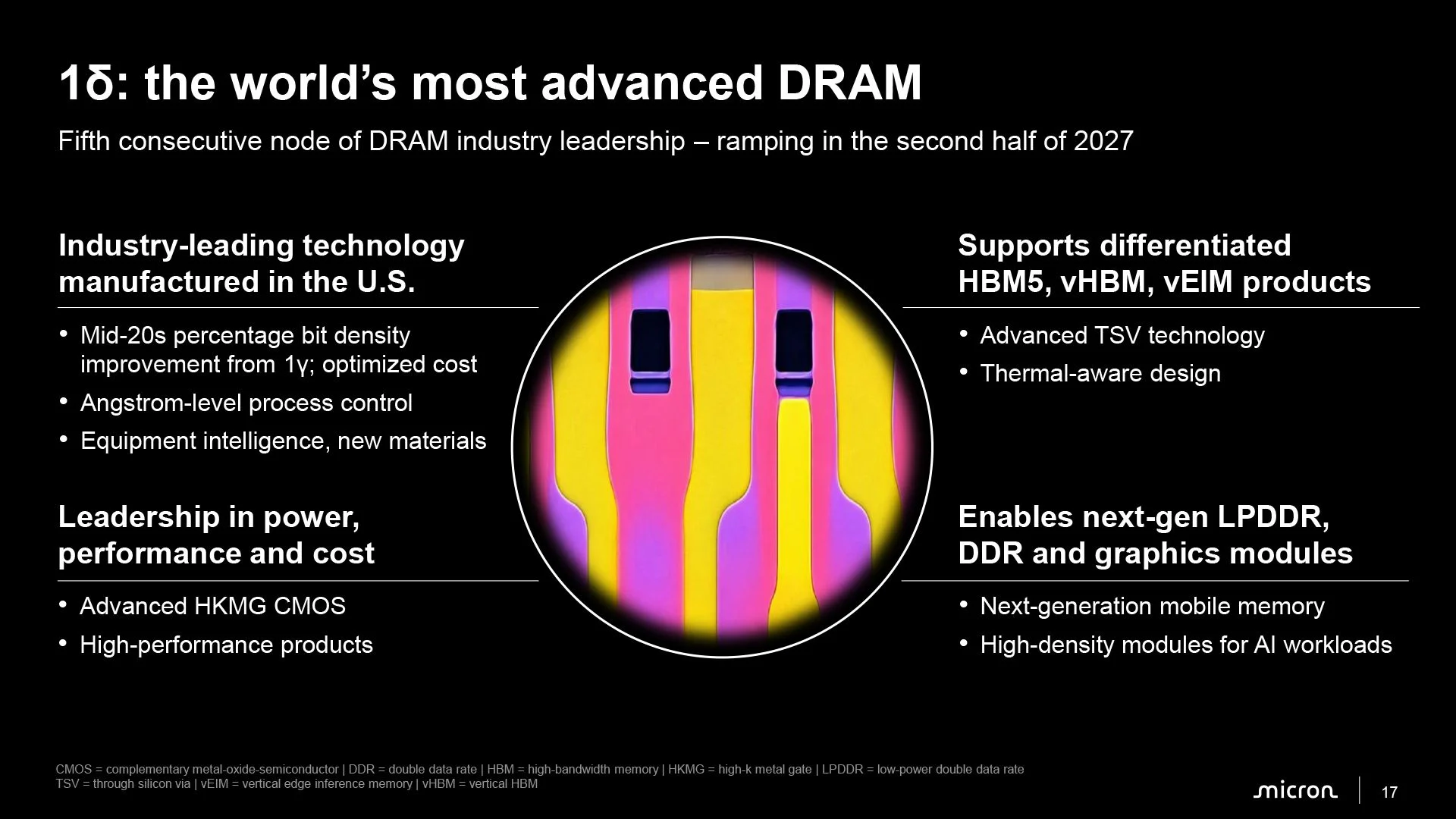
Micron’s 1γ process is already in high-volume production. Its successor, 1δ, is slated for volume production in the second half of 2027 and is expected to deliver a mid-20% increase in bit density. The node is designed with future AI memory products in mind, including HBM5, vHBM and vEIM.
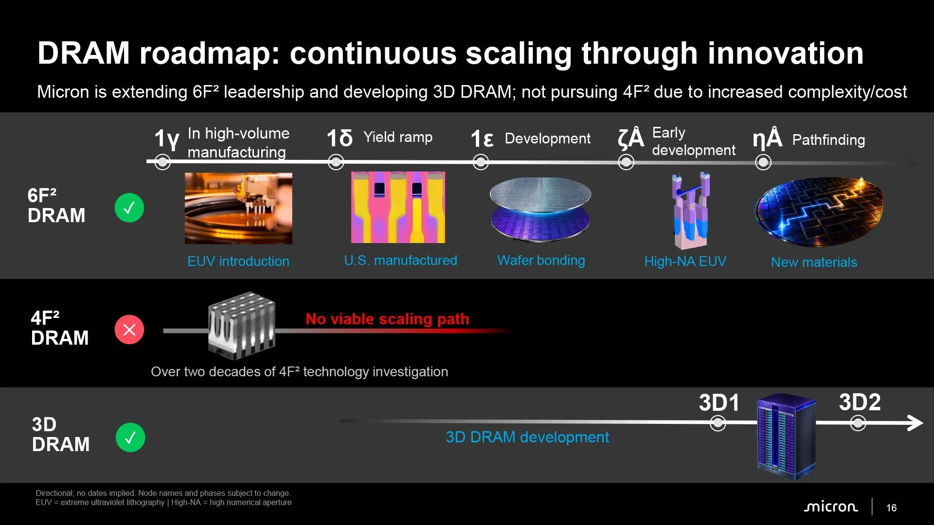
After 1δ, Micron plans to bring wafer bonding into its 1ε process, now under development. The company hasn’t shared how it will use the technique or what density, performance or cost gains it expects, so the practical impact remains an open question.
Farther out, the roadmap lists ζÅ, Micron’s first sub-10nm-class DRAM generation, and ηÅ, its second. Micron plans to use High-NA EUV lithography for ζÅ, then introduce new materials with ηÅ to keep reducing cell dimensions. Its work with Albany NanoTech is focused on advanced lithography research over the next five to 10 years; that effort is aimed at foundational technology that could eventually support DRAM manufacturing.
“Albany NanoTech, our announced focus on advanced lithography [is] really driving High-NA EUV roadmap for DRAM,” DeBoer said, describing the work as focused on the next five to 10 years.
Micron’s roadmap also includes two 3D DRAM generations, 3D1 and 3D2, but the company hasn’t disclosed their designs or timing. DeBoer described 3D DRAM as a parallel development path that Micron will adopt when it makes sense for manufacturing cost, complexity and device performance. That leaves the company room to develop stacked memory without committing to a launch before its trade-offs are clear.
Vertical memory moves closer to the processor
Micron is developing vertical HBM, vertical edge inference memory and custom HBM implementations. vHBM would place memory stacks on top of processors such as AI accelerators, shortening connections to pursue higher bandwidth and lower latency. But stacking memory above a processor also complicates cooling and restricts how many stacks can fit. Micron expects vHBM to supplement conventional HBM, which will continue to supply much of an accelerator’s memory capacity.
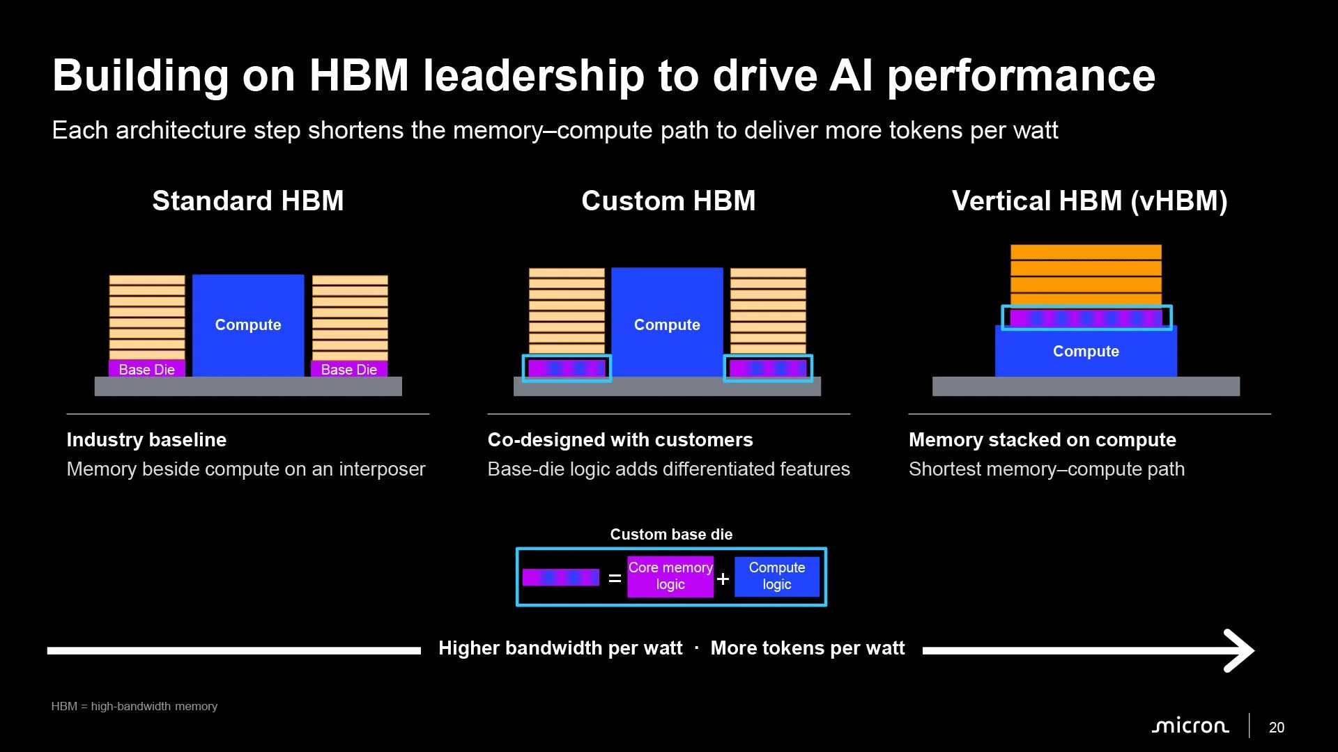
vEIM shares packaging and architectural traits with vHBM, but targets edge processors where energy use matters more than maximum bandwidth. Potential applications include autonomous vehicles and robotics. Micron’s first-generation target is 2 TB/s at less than 1 pJ per bit, comparable to the bandwidth cited for HBM4 running at 8 GT/s across a 2,048-bit interface. Micron says it will tailor capacity, bandwidth and power characteristics to customer needs.
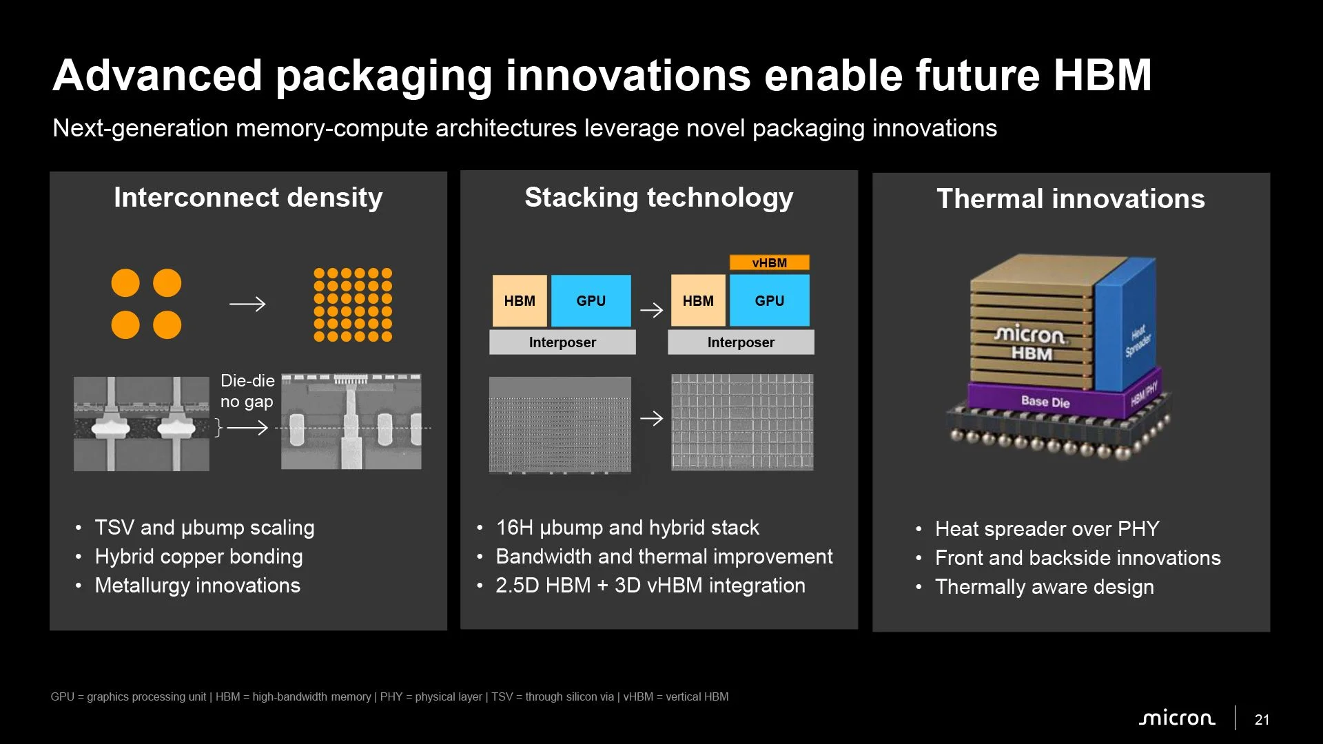
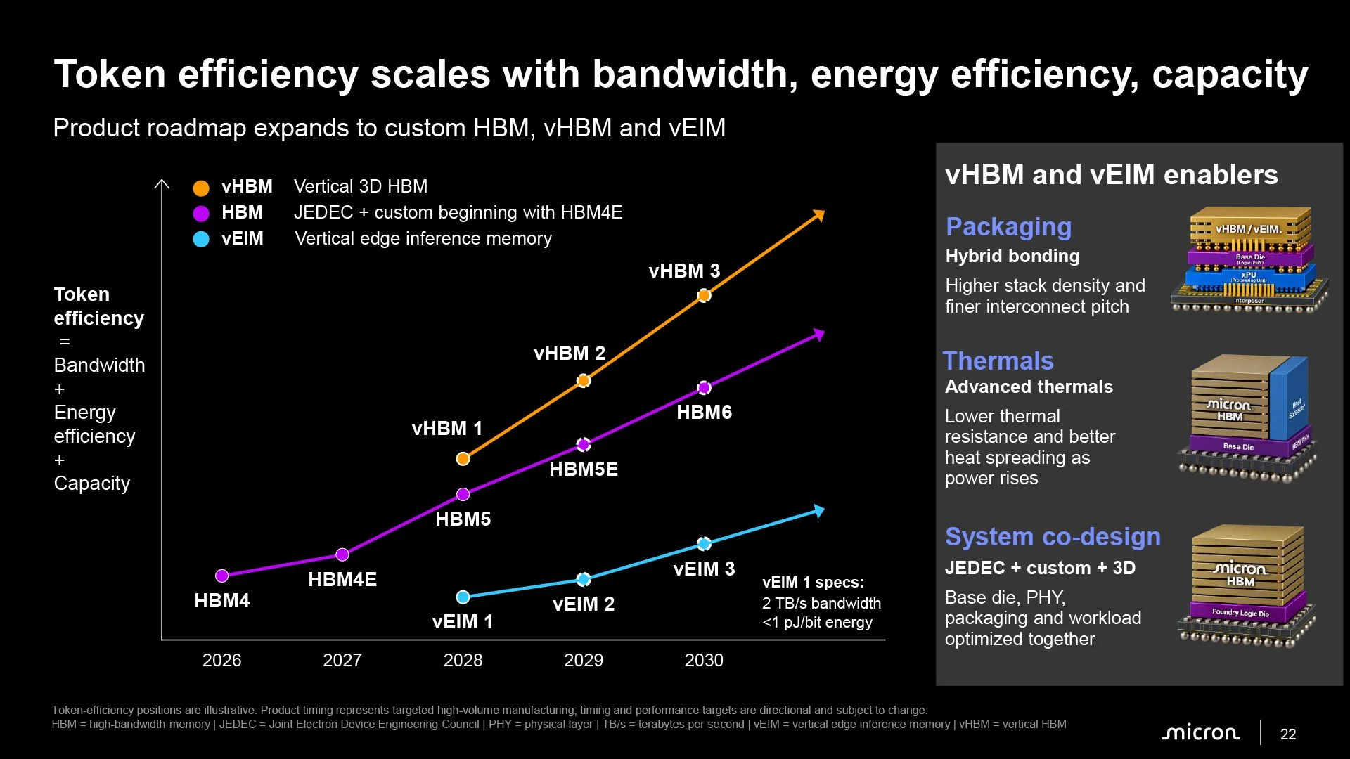
Both vertical designs depend on advanced packaging, especially hybrid bonding, which can create denser connections than conventional microbumps. Micron is also developing heat-spreading structures to move heat from hot regions of memory base dies through DRAM stacks, a particularly pressing challenge for vHBM.
Micron hasn’t announced production dates for vHBM, vEIM or cHBM. The direction is clear, though: as conventional cell scaling gets harder, memory performance will rely more on packaging and close coordination between memory and processor design. For system architects, memory is becoming a more integrated part of the ASIC rather than a component selected after the compute design is set.