Intel’s latest manufacturing update offers a clearer signal from Arizona than from Ohio: equipment installation has begun at Fab 62, putting the facility on a path to operation before the end of 2028. The company also confirmed High-NA EUV lithography is in high-volume manufacturing and reported a construction milestone at its Ohio complex, though key timelines and production plans remain undisclosed.
For Intel Foundry, the larger point is that domestic chip production depends on more than factory space. “There is an important difference between technologies made in America and technologies that are truly American-made,” Naga Chandrasekaran, Intel Foundry’s executive vice president and chief technology and operations officer, wrote. “The difference lies in the research and development process that transforms ideas into manufacturable technologies.”
Fab 62 moves from shell to equipment installation
Intel has completed the building shell at Fab 62 and is now installing production tools. The new facility will be the sixth high-volume semiconductor fab at the company’s Ocotillo campus in Arizona, a long-standing production hub that already houses advanced manufacturing, packaging, assembly, and testing operations.
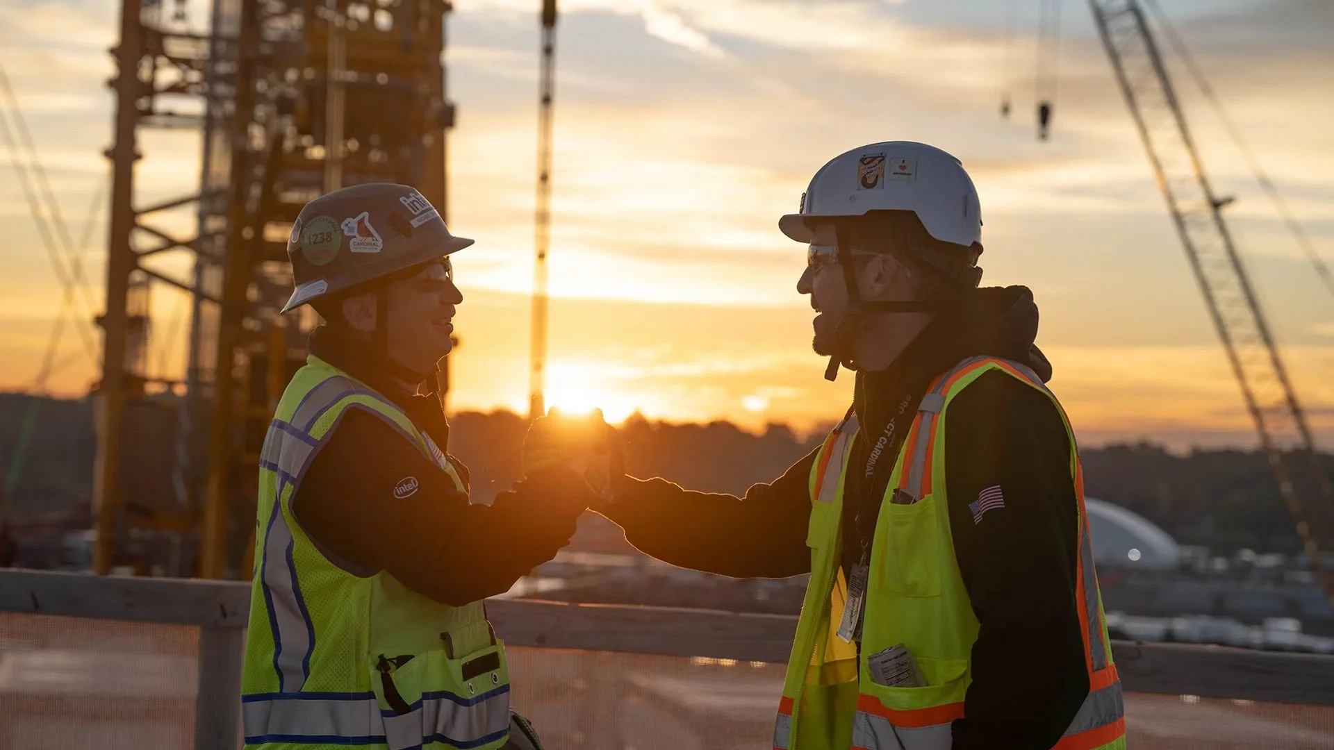
The process node for Fab 62 is still an open question. Intel has not assigned the site to Intel 14A, despite discussion of it as a possible location for the next-generation process. When Intel first announced Fab 52 and Fab 62, it said both would support its most advanced technologies, including Intel 20A and 18A. The company later designated Fab 52 for 18A production, leaving Fab 62 without a confirmed role.
Based on Intel’s process roadmap, Fab 62 could support Intel 18A, 18A-P, or 14A. Fab 52 already makes 18A chips nearby, so the new facility could add capacity for that process or support Intel’s move to 14A. Intel has not said which path it will take, how much wafer capacity the fab will provide, or what it will cost to complete.
Equipment installation does mark a meaningful step beyond construction of the shell. Intel expects Fab 62 to become operational before the end of 2028, but hasn’t specified when high-volume production will begin.
High-NA EUV reaches production use
Intel says it has integrated High-NA EUV lithography into high-volume manufacturing. The company was the first chipmaker to install a commercial High-NA EUV scanner, placing one at its D1X facility near Hillsboro, Oregon. Intel has used the technology to produce select tiles for Panther Lake processors and other chips.
D1X, part of Gordon Moore Park at Ronler Acres, develops Intel’s most advanced logic processes and starts production of new processors. Using High-NA EUV there gives Intel a way to evaluate the scanners in a production setting. The company hasn’t detailed how broadly it will use the technology or what performance benefits it has achieved.
For now, the available information suggests High-NA tools may be patterning some of the same circuits as Low-NA EUV systems. If so, their first production role may be to build manufacturing experience with the equipment, rather than to deliver a clear immediate advantage in chip design or output.
Ohio construction advances without a production date
At Intel’s Ohio One complex in New Albany, workers have installed the first major structural truss at the site’s first semiconductor fab. It’s a visible construction milestone, but Intel hasn’t supplied a revised schedule for the project or said when the facility will begin operating.
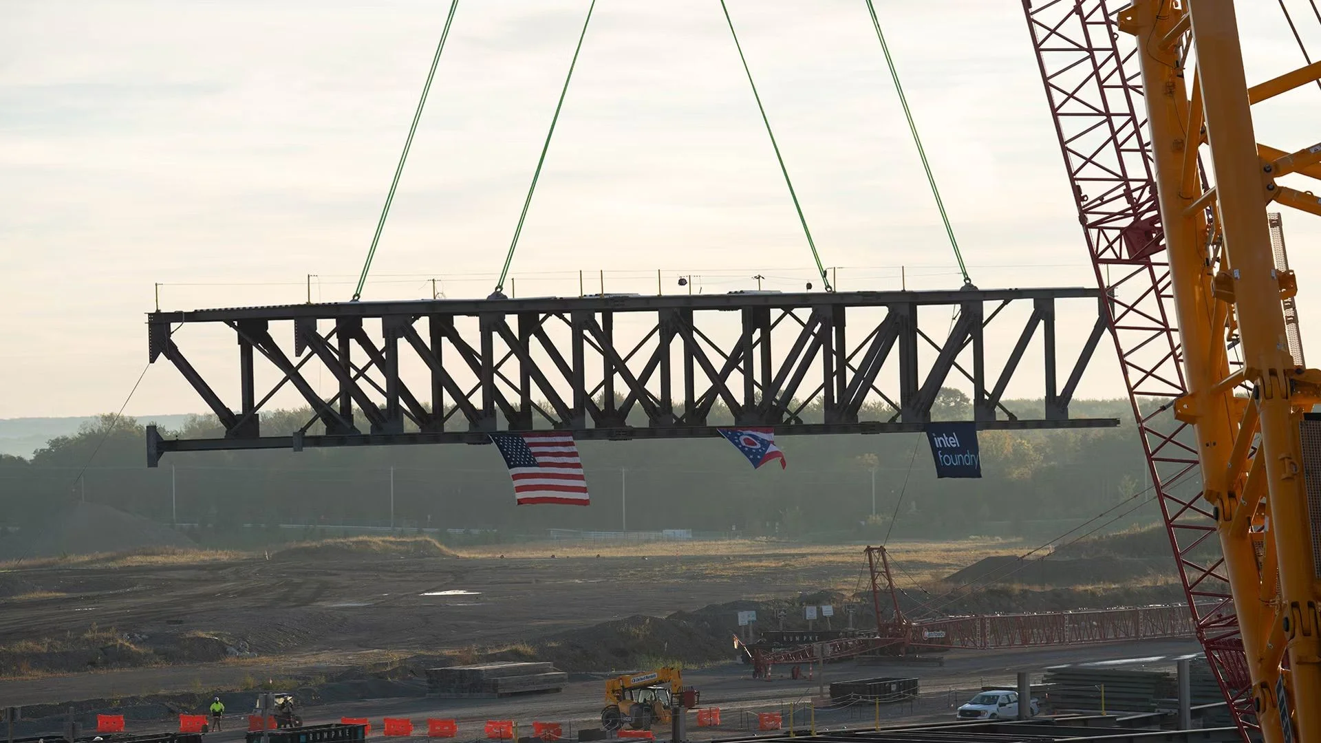
The company also hasn’t named the process technology planned for Ohio One or disclosed its expected manufacturing capacity. Those gaps make it difficult to judge when the complex will add to Intel’s chip output. For now, construction progress is the clearest update available.
Building out the U.S. production chain
Intel’s domestic footprint extends beyond wafer fabrication. Oregon is its main center for advanced logic and 3D interconnect research and development. Arizona supports advanced packaging research, assembly, and testing, while Intel’s New Mexico site produces complex multi-chiplet processors using packaging technologies ranging from EMIB to EMIB-T and Foveros.
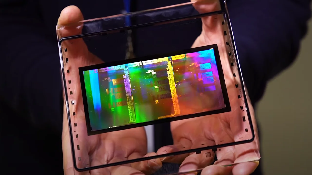
The company has also broken ground on a photomask manufacturing facility in Santa Clara, California. Photomasks are part of the chip production chain, and the project adds another domestic capability to Intel’s U.S. operations. Intel says more than 4,500 suppliers across 49 states support those operations, which account for annual U.S. spending of more than $29 billion.
Intel still relies on equipment from Europe and materials from Japan, but its investments span process research, manufacturing, packaging, and photomask production. The practical test for its expansion will be whether facilities such as Fab 62 and Ohio One reach production on schedule and deliver the capacity Intel has yet to disclose.