Micron’s decision to drop 4F² DRAM from its future plans reflects a broader engineering tradeoff: a smaller transistor footprint doesn’t automatically produce denser or cheaper memory. After roughly two decades of research, the company says capacitor dimensions and spacing remain the main constraints on DRAM density, while 4F² cells add manufacturing complexity and face limits as they scale.
That puts Micron on a different course from Samsung and SK hynix, whose roadmaps still include 4F² memory cells, according to TechInsights. Micron instead intends to keep shrinking conventional 6F² DRAM and eventually move toward vertically stacked 3D DRAM. Its position is that manufacturers can gain more from refining the process and capacitor geometry than from changing the transistor layout alone.
Why a smaller cell may not mean denser DRAM
The 4F² label describes a memory cell with an area equal to four times the square of the minimum lithographic feature size, or F. A conventional 6F² cell occupies six times F². If the two designs used identical feature dimensions and the cell area alone determined capacity, 4F² would take about one-third less space. In theory, that could allow 50% more cells in the same area.
But a DRAM cell is more than its transistor. Each cell also needs a capacitor to store data, and the capacitor’s size and spacing affect how tightly cells can be packed. Micron president and chief technology and products officer Scott DeBoer said capacitor pitch, rather than the transistor’s nominal footprint, sets the practical density limit. A smaller transistor may still need to sit beneath the same capacitor arrangement, so its reduced area may not translate into a smaller complete cell.
“It is important to understand the capacitor pitch, the capacitor size, and dimensions, is what sets the DRAM bit density, not whether it is 6F², 4F², 8F²,” DeBoer said at a company event on Wednesday. He described the supposed density advantage of 4F² over 6F² as “a bit of a myth,” arguing that cells built with different transistor structures must still fit within the limits imposed by capacitor pitch.
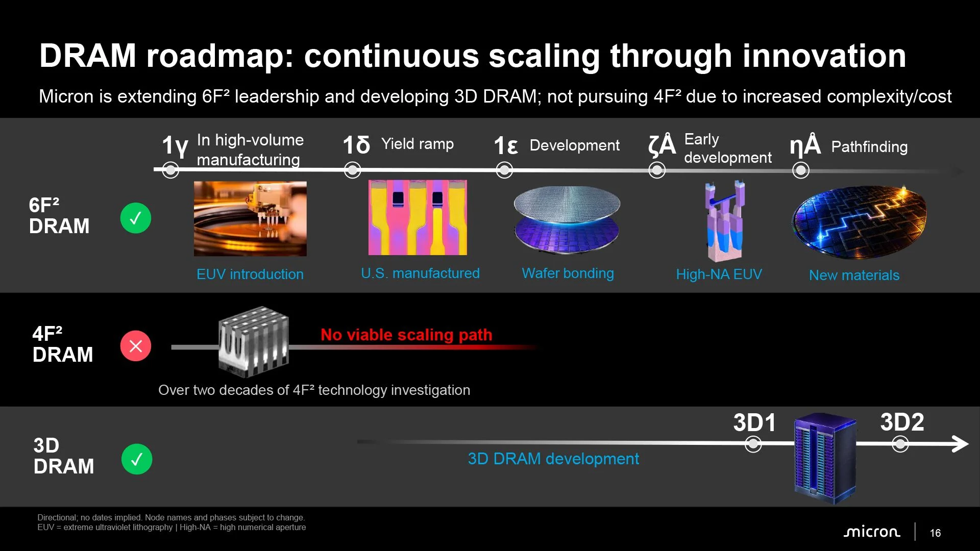
Micron says it has built experimental 4F² devices, so the company’s decision isn’t based on a claim that the architecture can’t be made. DeBoer said Micron invented 4F² DRAM and has assessed it over the past two decades. The issue, in his account, is whether the added steps and complexity justify the cost when the design doesn’t deliver a corresponding gain in bit density.
Micron’s near-term plan: keep shrinking 6F²
Micron plans to continue scaling conventional 6F² DRAM by reducing capacitor pitch and advancing process technology. The company points to lithography, new materials and wafer bonding as tools that could extend planar DRAM development for several more generations. That route keeps the focus on the dimensions that Micron says govern density, without adding a transistor architecture it believes brings limited practical benefit.
The company’s upcoming 1δ process is scheduled to enter volume production in the second half of 2027. Micron says it will deliver a mid-20% increase in bit density compared with the preceding generation. The company also plans to use High-NA EUV lithography in future DRAM generations.
This approach fits a pattern in Micron’s process choices. Several years ago, the company delayed integration of EUV lithography into its manufacturing flow while competitors adopted it earlier. Micron remained competitive on cost and performance, suggesting that it is willing to diverge from rivals when it sees a workable path through other process advances.
Scaling limits point toward 3D DRAM
Micron’s rejection of 4F² also reflects its view of the architecture’s longer-term prospects. DeBoer said manufacturers could build 4F² cells using process generations several nodes back, though doing so would be more complex and expensive. He argued that continued scaling would run into fundamental physical problems and eventually give way to 3D DRAM.
That distinction matters to the company’s roadmap. A process architecture that can be manufactured today may still be a poor bridge to future generations if its costs rise and its scaling path narrows. Micron appears to see 4F² as such an intermediate step: technically feasible, but with too little density upside to justify adopting it before another major architectural shift.
For 3D DRAM, the proposed change is to stack memory cells vertically, increasing density without relying only on smaller lateral dimensions. Micron is developing multiple generations of 3D DRAM production nodes alongside its next planar processes. It hasn’t announced when the architecture will reach commercial production. DeBoer said the company will make the transition when density, manufacturing complexity and cost align.
Samsung and SK hynix are still pursuing 4F², so the competing roadmaps will test different assumptions about where DRAM density gains will come from. Micron’s case is that the capacitor, rather than the transistor’s labeled cell area, sets the practical limit—and that work on 6F² processes can deliver more useful gains until vertical stacking is ready. For memory buyers and system designers, the next milestones to watch are the 1δ ramp and any details Micron shares about the cost and timing of 3D DRAM.