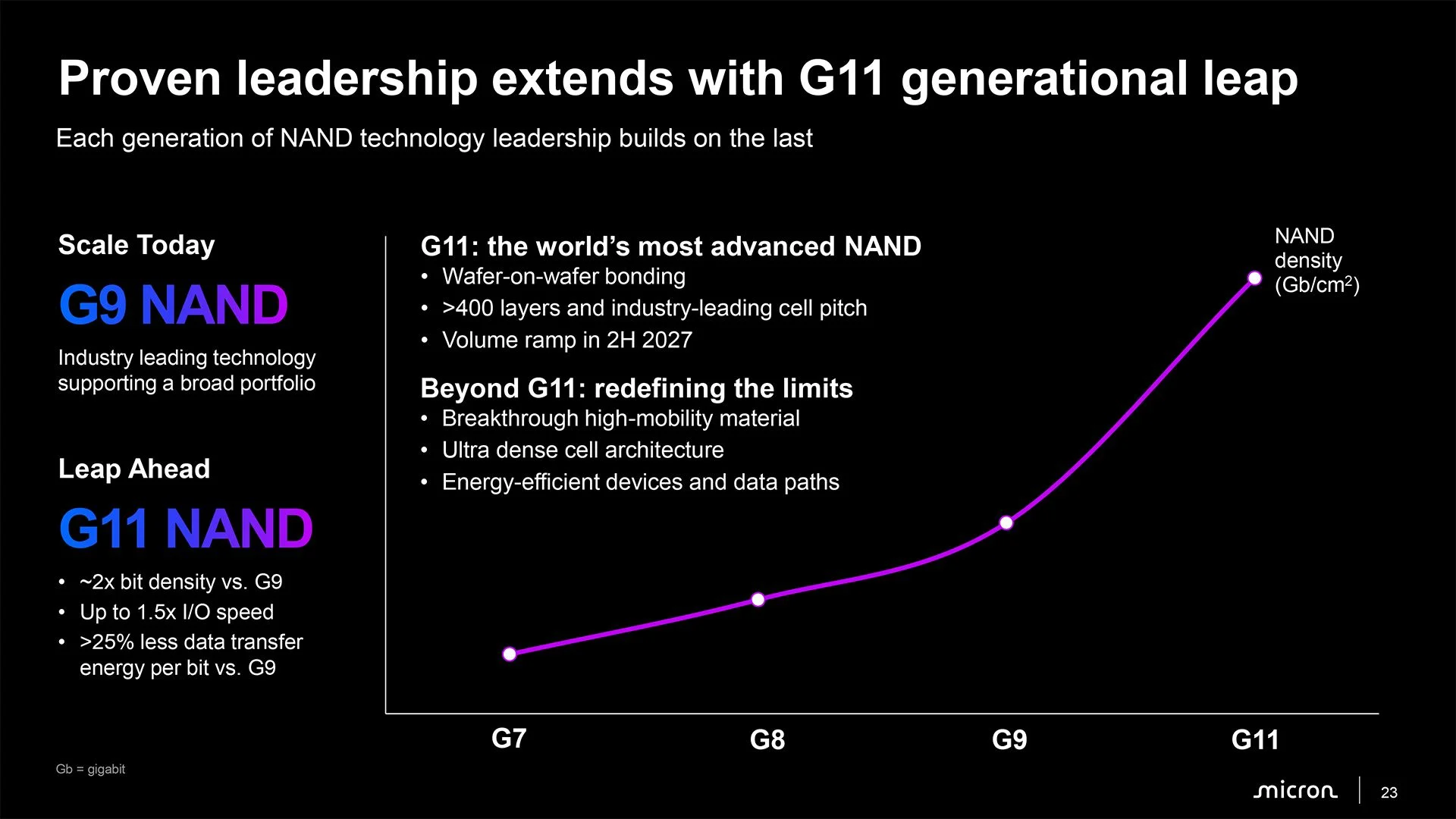
Micron’s next NAND generation is designed to raise storage density and I/O speed at the same time, while using less energy to transfer data. G11 is expected to enter mass production in the second half of 2027, with roughly twice the bit density of the company’s current G9 generation and I/O performance up to 50% higher. The approach combines more than 400 memory layers with wafer-on-wafer bonding, which lets Micron develop the memory array and its supporting logic separately.
Wafer bonding gives G11 room to scale
Scott DeBoer, Micron’s president and chief technology and products officer, described the timing as a matter of matching cost with product needs. “We had mentioned we will bring in wafer-on-wafer bonding technology at the right time when it’s cost-effective, and it brings in capability that is important for the product specs at the time, and this is the right timing for that technology,” he said at a company event this week. DeBoer called G11 “the world's most advanced NAND” and said it will ramp in the second half of 2027.
Micron’s stated density target is about 42 Gb/mm2 for 3D TLC, compared with 21 Gb/mm2 for G9. The company also projects data transfer energy per bit will fall by more than 25%. The source of the gains is not layer count alone: Micron says G11 will pair more than 400 layers with an industry-leading memory cell pitch. It hasn’t revealed the precise number of active wordline layers or memory decks.
Wafer-on-wafer bonding separates the fabrication of the NAND array from that of peripheral circuits and I/O. Micron can build each on a wafer using a process suited to that component, then bond the wafers together. The company already uses CMOS-under-array designs; bonding adds more freedom to tune the array and logic independently. If the process delivers as intended, that flexibility can support higher capacity and faster data movement.
Micron says G11’s I/O performance will improve by as much as 50% over G9. That could matter in high-capacity client and data center SSDs, as well as storage designed for AI workloads, where bandwidth and power efficiency both shape system performance. Micron hasn’t published the final G11 specifications, so the announced percentages remain targets rather than independently confirmed product results.
Beyond G11, scaling moves in three dimensions
Micron’s roadmap also points beyond adding layers. The company is working on high-mobility materials, denser cell architectures and more energy-efficient devices and data paths. Those efforts could improve transistor behavior, allow smaller memory cells and reduce the power spent moving data inside a NAND device.
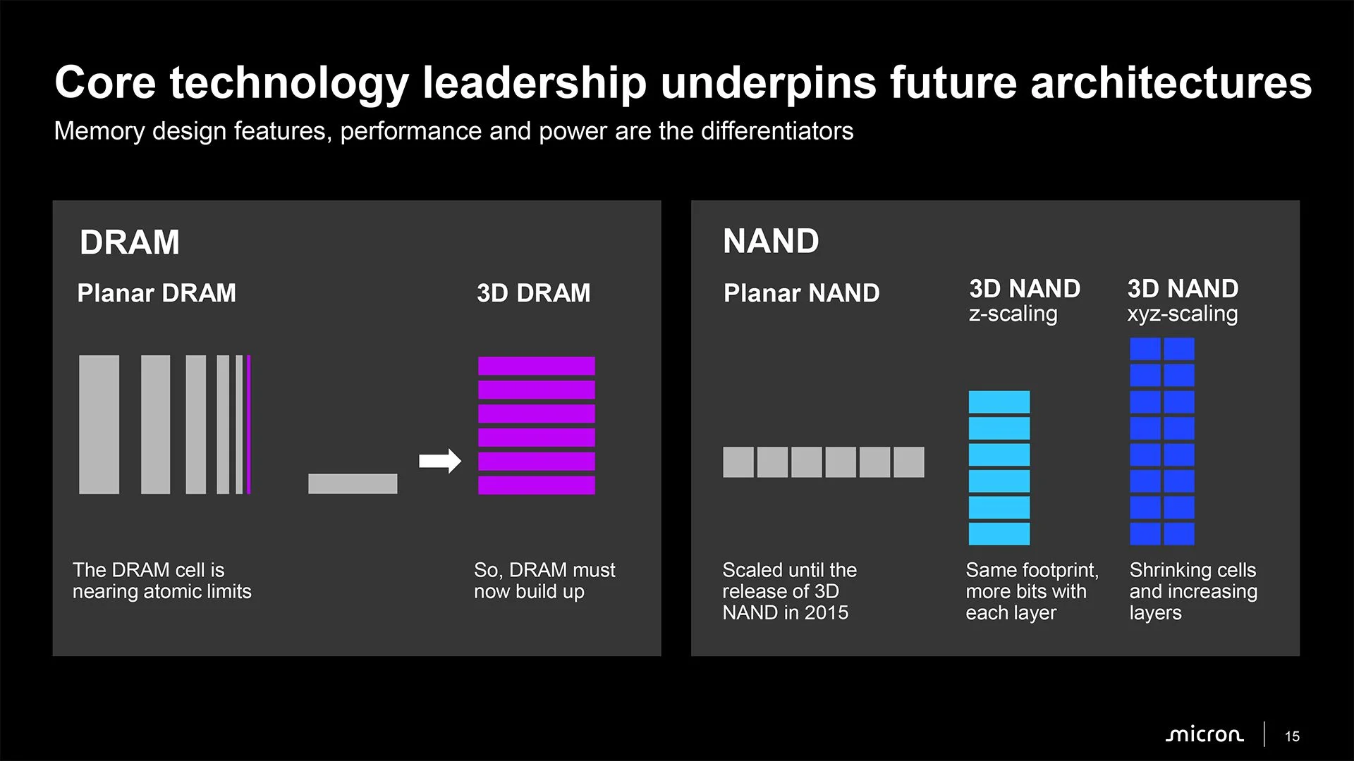
“Beyond G11, we have a strong roadmap, not going to go into great detail on it today, but really focused on new materials densifying the cell architecture, and continuing to focus on that XYZ scaling going forward,” DeBoer said. He added that the industry, including Micron, is pursuing density gains through both additional layers and smaller cell dimensions.
The company hasn’t shared density goals, architecture specifics or production dates for generations after G11. Its direction is clear, though: future gains will depend increasingly on cell geometry, materials and peripheral circuitry alongside layer counts. Micron expects to provide more detail on G11 in 2027, closer to high-volume production. For now, the key measure will be whether wafer bonding and tighter cells translate the roadmap’s density and efficiency targets into manufacturable products.